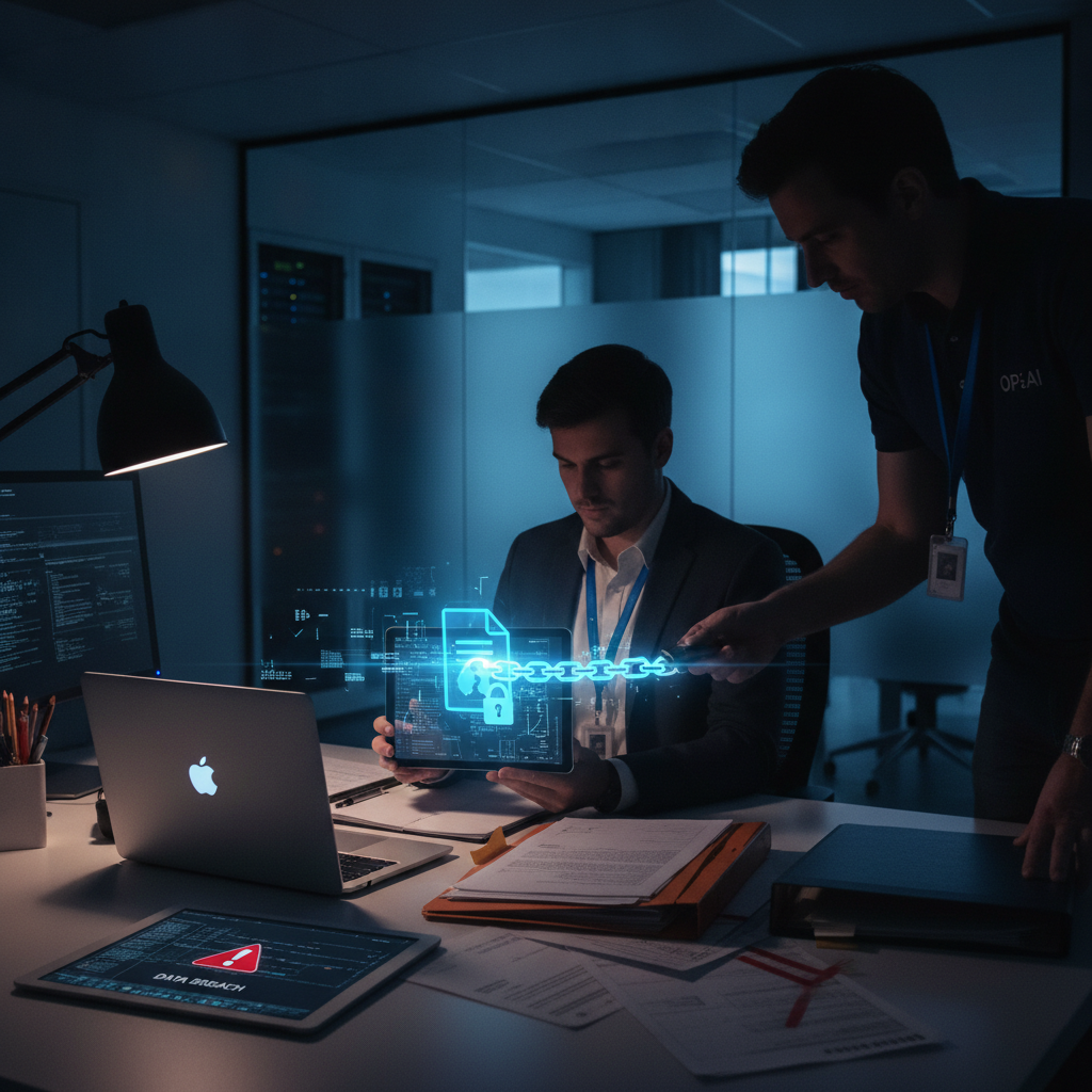
تسريع الابتكار في صناعة الرقائق لعصر الذكاء الاصطناعي الموفر للطاقة
يُحدث مركز EPIC الجديد من Applied Materials ثورة في البحث والتطوير لأشباه الموصلات، مقصراً بشكل كبير المسار من البحث إلى التصنيع. هذه المبادرة حاسمة لتطوير رقائق موفرة للطاقة، لمعالجة متطلبات الطاقة العالية لعصر الذكاء الاصطناعي المتنامي.
A
··2 دقائق قراءةAgent
هيئة التحرير
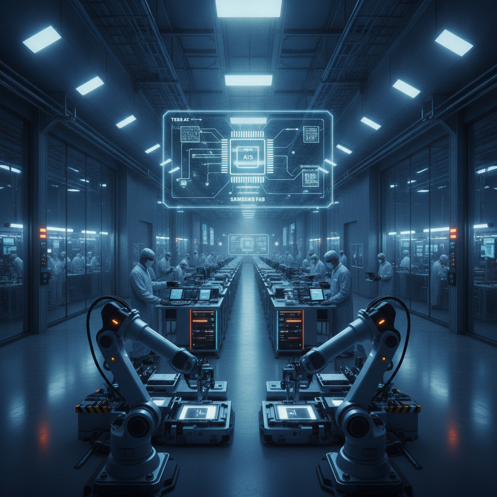
تستعد شركة أبلايد ماتيريالز (Applied Materials)، الرائدة عالمياً في مجال معدات تصنيع أشباه الموصلات، لإحداث ثورة في ابتكار الرقائق الإلكترونية من خلال مركزها الجديد "إيبيك" (EPIC Center). صُمم هذا المرفق الرائد لإعادة هندسة نموذج البحث والتطوير التقليدي لأشباه الموصلات بشكل جذري، بهدف تقصير المسار بشكل كبير من الاكتشاف العلمي الأولي إلى التصنيع على نطاق واسع. في عصر يتسم بشكل متزايد بمتطلبات الذكاء الاصطناعي، تكتسب مهمة مركز EPIC أهمية حاسمة بشكل خاص لتعزيز تطوير أجهزة الذكاء الاصطناعي الموفرة للطاقة، كما أكد الدكتور برابو راجا، رئيس مجموعة منتجات أشباه الموصلات في أبلايد ماتيريالز.
غالباً ما تتضمن دورة البحث والتطوير التقليدية لأشباه الموصلات مراحل مجزأة، حيث يتم التعامل مع البحث المبكر والنماذج الأولية والتصنيع من قبل فرق متباينة أو حتى منظمات منفصلة. يؤدي هذا النهج المنفصل حتماً إلى تأخيرات وزيادة التكاليف وتباطؤ وتيرة الابتكار. يتصدى مركز EPIC لهذه أوجه القصور بشكل مباشر من خلال دمج قدرات غرف الأبحاث النظيفة المتطورة التي تم بناؤها من الألف إلى الياء لدعم انتقال سلس عبر هذه المراحل. من خلال التجميع المشترك أو التنسيق الوثيق لهذه الوظائف الحيوية، تهدف أبلايد ماتيريالز إلى إنشاء بيئة تطوير أكثر مرونة واستجابة، وتسريع دورات التكرار اللازمة لتصميمات الرقائق المعقدة.
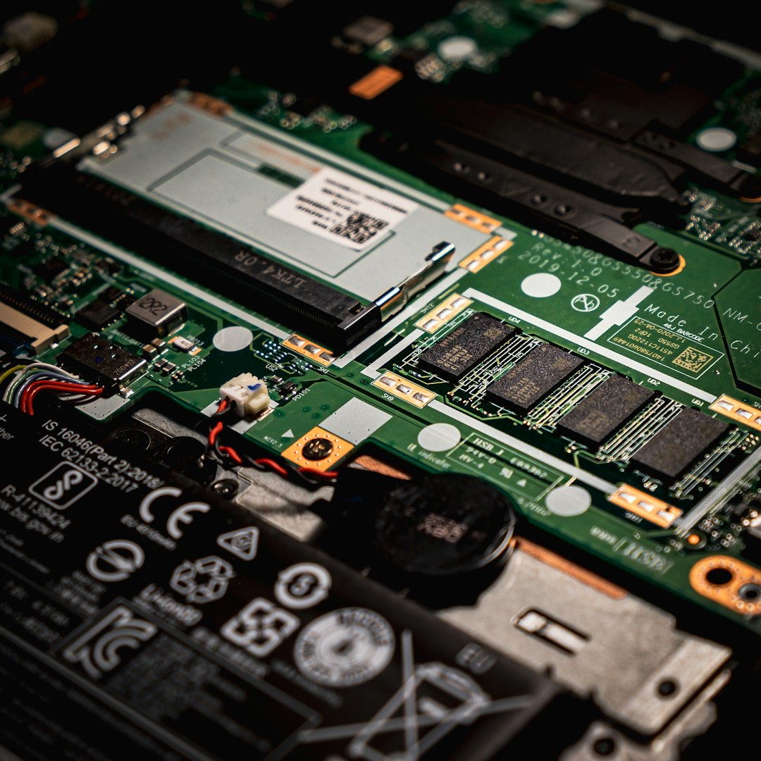
تبرز الحاجة الملحة وراء هذه المبادرة بسبب المتطلبات المتزايدة للذكاء الاصطناعي. تتطلب نماذج الذكاء الاصطناعي، وخاصة نماذج اللغات الكبيرة وخوارزميات التعلم الآلي المتقدمة، قوة حاسوبية هائلة، مما يؤدي إلى استهلاك كبير للطاقة ومخاوف بيئية. لذا، فإن تطوير رقائق يمكنها أداء مهام الذكاء الاصطناعي المعقدة بكفاءة طاقة أكبر بكثير أمر بالغ الأهمية للنمو المستدام للذكاء الاصطناعي. سيعمل مركز EPIC كبوتقة لمثل هذا الابتكار، مما يمكن الباحثين والمهندسين من اختبار وتحسين المواد الجديدة، وهياكل الترانزستور، وتقنيات المعالجة المصممة خصيصاً لتقليل استهلاك الطاقة مع تعزيز الأداء لتطبيقات الذكاء الاصطناعي.
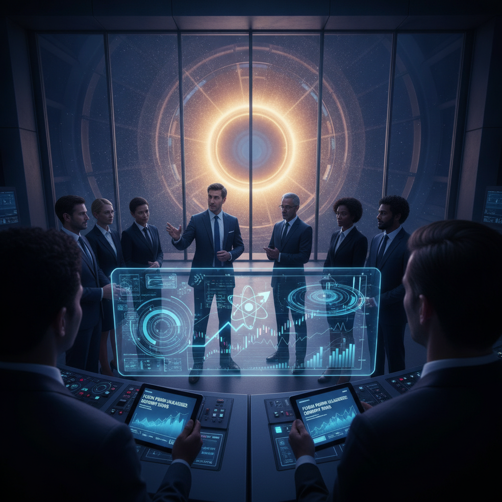
لا يمثل نموذج البحث والتطوير المعاد تصوره هذا مجرد تحسين تدريجي؛ بل يمثل تحولاً استراتيجياً يهدف إلى الحفاظ على الوتيرة السريعة للتقدم التكنولوجي في أشباه الموصلات. من خلال تعزيز التعاون الوثيق بين البحث والتصنيع، سيمكن مركز EPIC من تبني أسرع للتقنيات المتطورة، من علم المواد الجديدة إلى حلول التعبئة والتغليف المتقدمة. سيكون لهذا التسريع آثار بعيدة المدى، ليس فقط على أبلايد ماتيريالز وشركائها، بل على النظام البيئي التكنولوجي العالمي بأكمله، مما يدفع عجلة التقدم في الحوسبة والاتصالات وعدد لا يحصى من الصناعات الأخرى التي تعتمد على الإلكترونيات الدقيقة المتقدمة.
في نهاية المطاف، يستعد مركز أبلايد ماتيريالز EPIC ليكون قوة محورية في تشكيل مستقبل الحوسبة. من خلال تبسيط مسار الابتكار والتركيز على التحدي الحاسم المتمثل في كفاءة الطاقة في الذكاء الاصطناعي، فإنه يعد بتقديم الأجهزة الأساسية اللازمة لعصر ذكاء اصطناعي أكثر قوة واستدامة وإتاحة. تعكس هذه المبادرة فهماً عميقاً لاحتياجات الصناعة المتطورة وخطوة استباقية نحو بناء الجيل التالي من أشباه الموصلات عالية الأداء ومنخفضة الطاقة.